
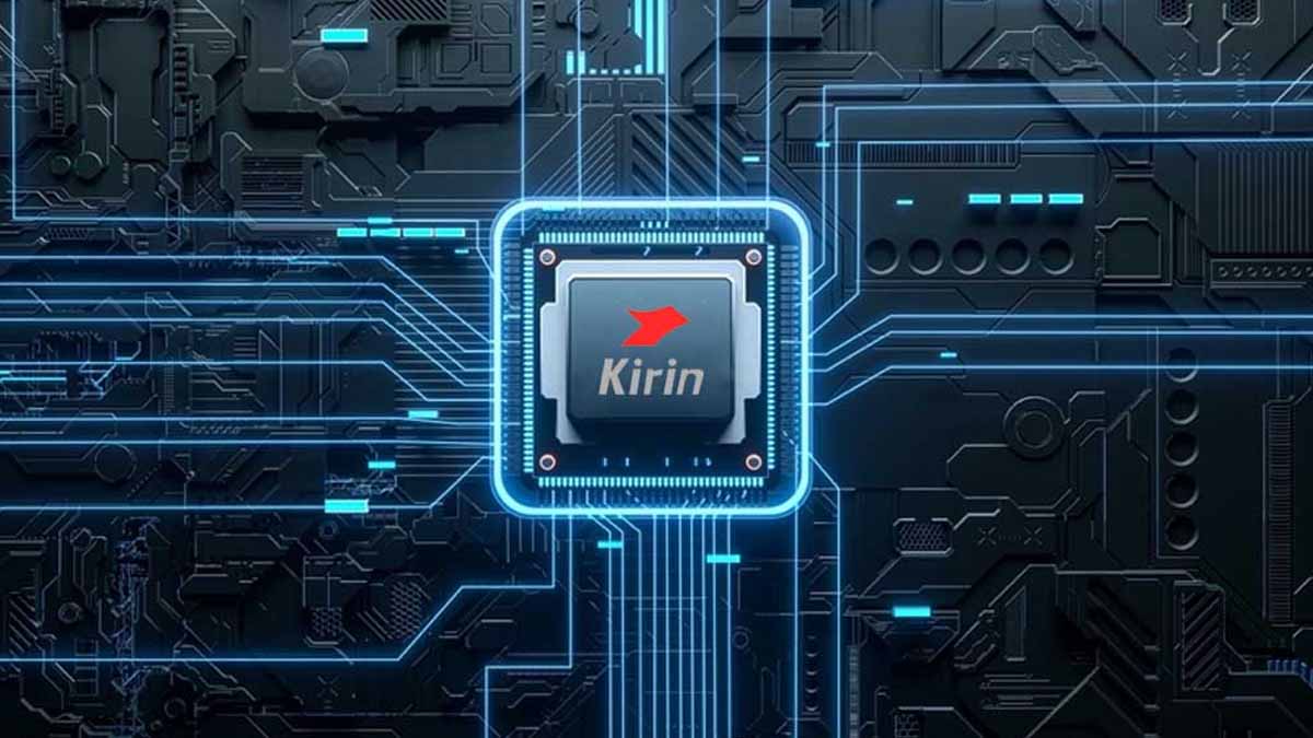
Huawei is pushing forward with a new semiconductor strategy despite ongoing US export restrictions, announcing a design technique called LogicFolding that it plans to implement in its next generation of Kirin smartphone chips this fall. The approach, presented by Huawei semiconductor president Tingbo He at a Shanghai conference, involves stacking logic layers to improve efficiency and transistor interaction, essentially expanding from a single layer to two.
This development carries weight in the global chip race. For Nvidia, already constrained by American limits on selling advanced processors in China, it narrows the window for high-end AI chip sales even further. Apple also faces renewed pressure in the world’s second-largest smartphone market, where Huawei’s Mate 60 series demonstrated the company’s ability to regain ground through domestic technology breakthroughs. Beijing’s broader push for self-reliance in semiconductors has taken on greater urgency amid geopolitical tensions, turning Huawei into a symbol of both resilience and restriction.
Huawei claims its method could eventually achieve performance equivalent to 1.4-nanometer manufacturing by 2031. For context, industry leader TSMC has only recently moved into volume production of 2-nanometer chips. The company has branded the concept as the “Law of Tau” or τ scaling, positioning it as a systems-level response to the slowing of traditional Moore’s Law, which for decades predicted transistor counts doubling roughly every two years. Huawei says it has already designed and produced 381 chips based on this principle over the past six years.
Yet analysts remain cautious about the claims. Experts note that while folded or stacked designs can deliver density gains, they do not automatically resolve deeper challenges around manufacturing yields, power consumption, heat management, and overall device performance. True 1.4 nm-class production involves complex issues that go beyond architectural tweaks. Huawei itself acknowledges this remains a long-term effort, potentially spanning a decade, and scaling the technology from smartphones to demanding AI data centers would represent the real test of its viability.
The situation reflects broader industry realities. US sanctions have blocked Huawei from accessing cutting-edge EUV lithography equipment, forcing alternative paths that introduce packaging complexities and thermal constraints. These workarounds can work in consumer devices but often struggle at scale. Nvidia’s CEO recently conceded ground in China to local players, highlighting how export controls have reshaped competitive dynamics without fully halting progress.
In many ways, Huawei’s announcement fits a pattern of incremental innovation under pressure rather than a clean breakthrough. The semiconductor sector has long grappled with physical limits as nodes shrink, leading companies to explore 3D stacking and co-design strategies. Whether LogicFolding delivers meaningful advantages in real-world products like the upcoming Mate 90 series will depend on execution, not presentation. For now, it underscores China’s determination to reduce dependence on foreign technology, even as questions linger about the gap between ambition and mass-production reliability.